 Gordon Moore might not have thought that this day would come when his popular “Moore’s law” will see some serious irrelevance.
“number of transistors that can be placed inexpensively on an integrated circuit has doubled approximately every two years”
Over the years scientists and chip industry evangelists have argued that Moore’s law is still valid as we enter the era of Multi-core processors. But, the latest revelation from IBM can give the the Moore’s law a permanent backseat. IBM’s technology takes a step backward (by creating 6x times bigger transistor) and still a giant-leap ahead (by creating much higher Operating clock and hence the speed).
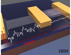
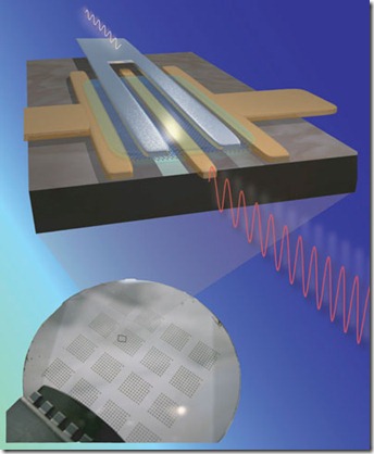
IBM researchers have made a breakthrough in the development of ultra-high-speed transistor design, creating a 100GHz graphene-based wafer-scale device. What this means is that they manufactured a whole wafer of the the things at once, rather than one researcher hovering over a microscope to painstakingly construct one or a handful of transistors.
The transistor that the researchers have developed is a relatively large one, with a gate length of 240nm (a typical desktop processor is 45nm) – speeds should increase as the gate length shrinks. Hence, 100Ghz is just the beginning.
The FET (field-effect transistor) that the IBM team developed exploits “very high carrier mobilities” of graphene based on a paper published in the journal Science. It employs a one-atom-thick sheet of carbon atoms grown on a silicon substrate.
The high carrier mobility of graphene has been exploited in field-effect transistors that operate at high frequencies. Transistors were fabricated on epitaxial graphene synthesized on the silicon face of a silicon carbide wafer, achieving a cutoff frequency of 100 gigahertz for a gate length of 240 nanometers. The high-frequency performance of these epitaxial graphene transistors exceeds that of state-of-the-art silicon transistors of the same gate length.
This extraordinarily thin sheet is created in an ordered crystaline structure on top of another crystaline structure (ol’ garden-variety silicon). The graphene sheet has a hexagonal, honeycombed structure.
A long gate length means plenty of room for speed improvements
Why Graphene?
In Contrast with Silicon, Graphene has an exceptional electron mobility, but it has remained stubbornly resistant to the creation of band gaps — the electron-free zones necessary for transistors to funtion as on/off switches. And IBM’s research team made this possible.
In an IBM Research statement, vice president for science and technology, said:
“A key advantage of graphene lies in the very high speeds in which electrons propagate, which is essential for achieving high-speed, high-performance next generation transistors. The breakthrough we are announcing demonstrates clearly that graphene can be utilized to produce high performance devices and integrated circuits.”
Key to the breakthrough is what the paper calls a “interfacial polymer layer” that separates the graphene sheet from its metal gate dialectric. And although the gate length is a hefty 240nm, IBM notes that there is “plenty of space for further optimization of its performance by scaling down the gate length.”
But even at this gate length and at this early stage of their development, IBM’s graphene transistors can already achieve speeds of 250 percent (i.e. 100Ghz) of those achievable by “state-of-the-art” silicon metal-oxide semiconductor FETs of the same gate length (40Ghz).
Notably, there are two breakthroughs this processor prototype will go through:
- All test were conducted at room temperature. IBM claims if this is done at a lower temperature, performance can be scaled to much higher levels (roughly 40%)
- Gate size: Right now the gate size is 240nm nearly 6x times more than current generation PCs. As the research advances, these graphene chips can be compressed further thereby reducing the distance and delay, improving the performance multiple times.
We write Latest in Hardware, Research, Gadgets: Android, iPhone, Apple, Google and Tech Guides, Tech News @taranfx on Twitter and:
loading...
loading...


Is the author suggesting that because the graphene design is using 240nm tech – it can be scaled up quickly as we know how to use 45nm tech (I heard 25nm is now functional). So does that equate to 800Ghz (1 Thz?!) in a couple of years? Kurzweil still on track then?
loading...
loading...